
Product Concept
Enatsys Design proposes a new design methodology and tools for the power budgeting and SI analysis flow in early design stage. The proposed solution consists of mixed-level design explorer, power estimator, interactive power specification editor, IO PAD design rule checker, comprehensive floorplan editor, power network analyzer and hierarchical layout viewer. The main objective of this design automation solution is to enable SoC designer to achieve the first silicon success with minimum design turn around time. The key benefits of these tools are to eliminate the unnecessary design iteration with fast and accurate prediction and efficient prevention of the power and SI related design errors at earlier design stage.
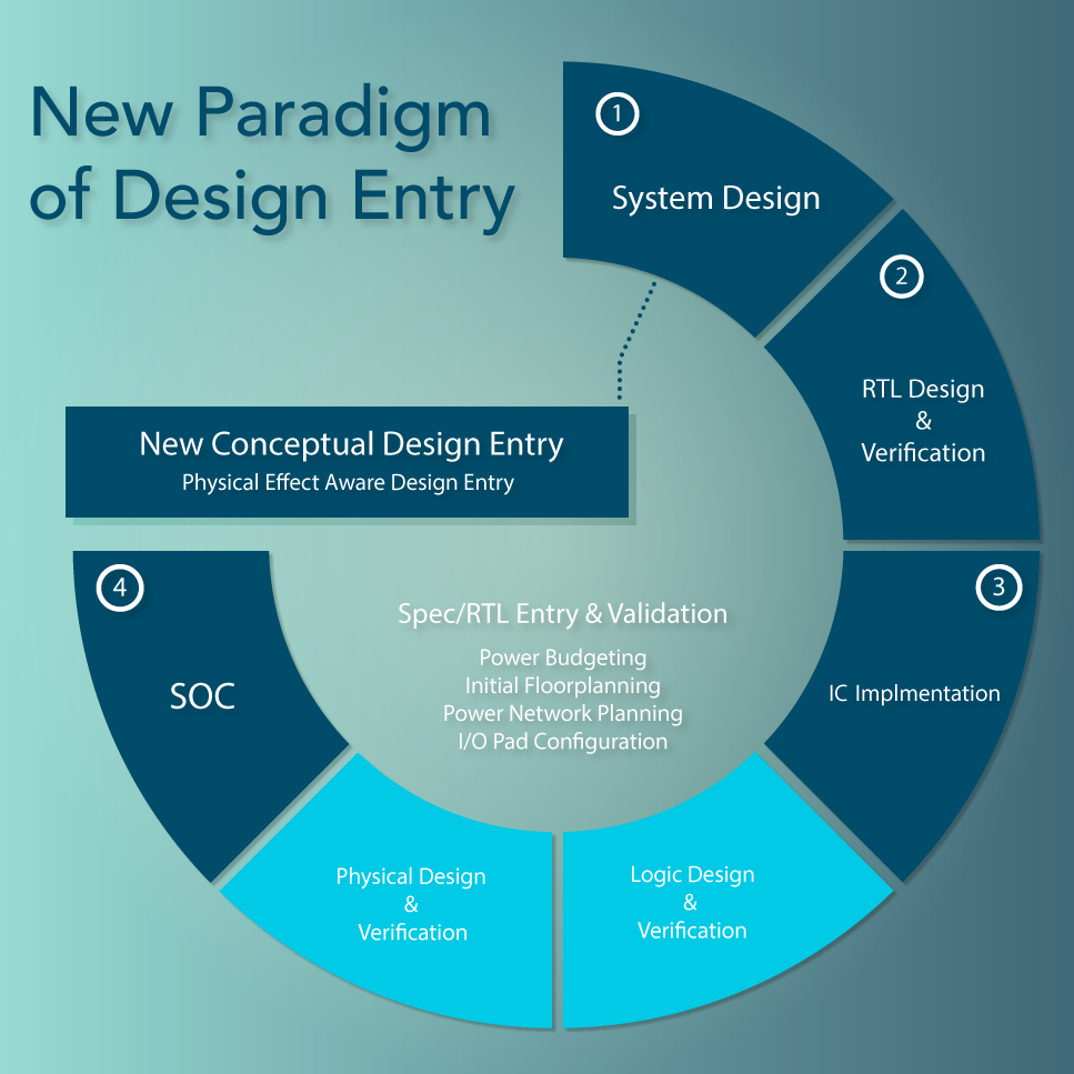
In general SoC design flow, the cost to find and fix the SI problems is extremely high because the verification tasks for the SI problems are performing at the backend design stage. Most of the design rule violations of SI and power issues are relating to each others and it's not easy to define the actual cause of the problem. As the complexity of the chip is increased and smaller process technology is used in SoC design, the analysis and verification time for the SI issues is the critical factor to achieve the faster design TAT. The IC implementation methodology is the most significant effort to eliminate the inconsistency of the analysis or verification results of different point tools and manage the design constraints consistently from the RTL description to mask layout data generation. However the brand new IC implementation tools are not enough to handle all the needs to analysis and verify the design constraints which related with SI issues in real SoC design world, because most of the SoC designs contain the IP blocks and the IC implementation tools have a limitation to see inside of them. In some designs, it is possible to achieve the design closure with IC implementation methodology but in many cases it's very difficult to keep timing constraint of the design delivered from logic synthesis stage to physical layout stage. The excessive voltage drop of the power network is one of the causes of the inaccurate timing analysis at post layout verfication stage because it causes an extra delay of logic blocks. The extra design iterations are nightmare for SoC designers. Prediction and prevention of the power and SI issues are the keys to avoid the painful tasks to find and fix the design errors at the final stage of the design. Entasys Design proposes a methodology independent tool for early design stage power budgeting and SI analysis. The major benefit of this solution is the minimization of the design TAT with efficient power budgeting and SI analysis in early design stages. The IC implementation methodology is the major trend in SoC design automation but it's just a part of the design methodology in real SoC design world.